(China (Mainland))

Product Summary
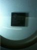
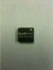
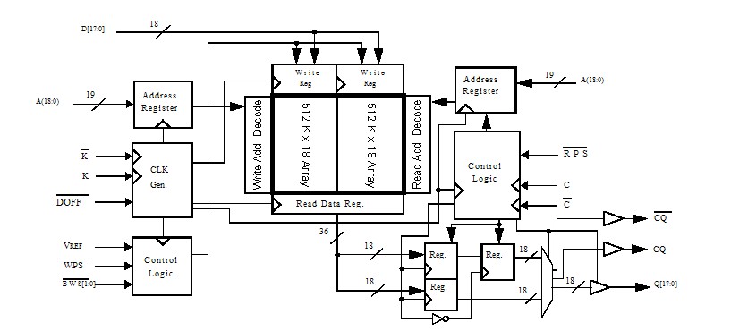
The CY7C1312KV18-250BZC is a 1.8 V Synchronous Pipelined SRAM, equipped with QDR IIarchitecture. QDR II architecture consists of two separate ports:the read port and the write port to access the memory array. The CY7C1312KV18-250BZC has dedicated data outputs to support read operationsand the write port has dedicated data inputs to support writeoperations. All synchronous inputs pass through input registers controlled bythe K or K input clocks. All data outputs pass through outputregisters controlled by the C or C (or K or K in a single clockdomain) input clocks. Writes are conducted with on-chipsynchronous self-timed write circuitry.
Parametrics
CY7C1312KV18-250BZC absolute maximum ratings: (1)Storage temperature : –65 °C to +150 °C; (2)Ambient temperature with power applied: –55 °C to +125 °C; (3)Supply voltage on VDD relative to GND: –0.5 V to +2.9 V; (4)Supply voltage on VDDQ relative to GND: –0.5 V to +VDD; (5)DC applied to outputs in High Z : –0.5 V to VDDQ + 0.5 VDC; (6)input voltage[17] : –0.5 V to VDD + 0.5 V; (7)Current into outputs (LOW): 20 mA; (8)Static discharge voltage (MIL-STD-883, M. 3015): > 2001 V; (9)Latch up current: > 200 mA.
Features
CY7C1312KV18-250BZC features: (1)Echo clocks (CQ and CQ)simplify data capture in high-speedsystems; (2)Single multiplexed address input bus latches address inputsfor both read and write ports; (3)Separate port selects for depth expansion; (4)Synchronous internally self-timed writes; (5)QDR II operates with 1.5 cycle read latency when DOFF isasserted HIGH; (6)Operates similar to QDR I device with one cycle read latencywhen DOFF is asserted LOW; (7)Available in ×8, ×9, ×18, and ×36 configurations; (8)Full data coherency, providing most current data; (9)Core VDD = 1.8 V (±0.1 V); I/O VDDQ = 1.4 V to VDD Supports both 1.5 V and 1.8 V I/O supply; (10)Available in 165-ball FBGA package (13 × 15 × 1.4 mm); (11)Offered in both Pb-free and non Pb-free packages; (12)Variable drive HSTL output buffers; (13)JTAG 1149.1 compatible test access port; (14)PLL for accurate data placement.
Diagrams
| Image | Part No | Mfg | Description |  |
Pricing (USD) |
Quantity | ||||||||||||
|---|---|---|---|---|---|---|---|---|---|---|---|---|---|---|---|---|---|---|
 |
 CY7C1312KV18-250BZC |
Cypress Semiconductor |
SRAM 18432KB 1ms 560mA |
Data Sheet |
|
|
||||||||||||
|
CY7C1312KV18-250BZCT |
Cypress Semiconductor |
SRAM 18432KB 1ms 560mA |
Data Sheet |
|
|
||||||||||||