(China (Mainland))

Product Summary
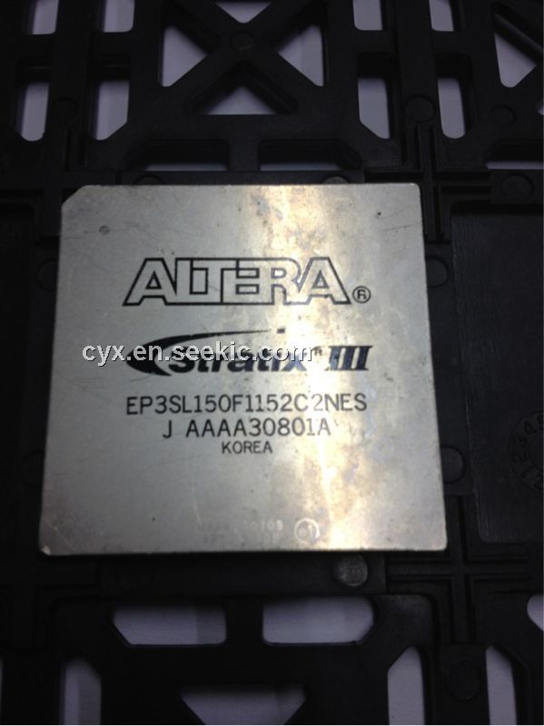
The EP3SL150F1152C2NESJ is a FPGA. The EP3SL150F1152C2NESJ provides one of the most architecturally advanced, high-performance, low-power FPGAs in the marketplace. The EP3SL150F1152C2NESJ lower power consumption through Altera innovative Programmable Power Technology, which provides the ability to turn on the performance where needed and turn down the power consumption for blocks not in use. Selectable Core Voltage and the latest in silicon process optimizations are also employed to deliver the industry lowest power, high-performance FPGAs.
Parametrics
EP3SL150F1152C2NESJ absolute maximum ratings:(1)Selectable core voltage power supply, VCCL: -0.5 to 1.65 V; (2)I/O registers power supply, VCC: -0.5 to 1.65 V; (3)Phase-locked loop (PLL) digital power supply, VCCD_PLL: -0.5 to 1.65 V; (4)analog power supply, VCCA_PLL PLL: -0.5 to 3.75V; (5)Programmable power technology power supply, VCCPT: -0.5 to 3.75V; (6)Configuration pins power supply, VCCPGM: -0.5 to 3.9V; (7)I/O pre-driver power supply, VCCPD: -0.5 to 3.9V; (8)I/O power supply, VCCIO: -0.5 to 3.9V.
Features
EP3SL150F1152C2NESJ features:(1)48,000 to 338,000 equivalent logic elements (LEs); (2)2,430 to 20,497 Kbits of enhanced TriMatrix memory consisting of three RAM block sizes to implement true dual-port memory and FIFO buffers; (3)High-speed DSP blocks provide dedicated implementation of 9×9, 12×12, 18×18, and 36×36 multipliers (at up to 550 MHz), multiply-accumulate functions, and finite impulse response (FIR) filters; (4)I/O:GND:PWR ratio of 8:1:1 along with on-die and on-package decoupling for robust signal integrity; (5)Programmable Power Technology, which minimizes power while maximizing device performance; (6)Selectable Core Voltage, available in low-voltage devices (L ordering code suffix), enables selection of lowest power or highest performance operation; (7)Up to 16 global clocks, 88 regional clocks, and 116 peripheral clocks per device; (8)Up to 12 phase-locked loops (PLLs) per device that support PLL reconfiguration, clock switchover, programmable bandwidth, clock synthesis, and dynamic phase shifting; (9)Memory interface support with dedicated DQS logic on all I/O banks; (10)Support for high-speed external memory interfaces including DDR, DDR2, DDR3 SDRAM, RLDRAM II, QDR II, and QDR II+ SRAM on up to 24 modular I/O banks; (11)Up to 1,104 user I/O pins arranged in 24 modular I/O banks that support a wide range of industry I/O standards; (12)Dynamic On-Chip Termination (OCT) with auto calibration support on all I/O banks; (13)High-speed differential I/O support with serializer/deserializer (SERDES) and dynamic phase alignment (DPA) circuitry for 1.6 Gbps performance.
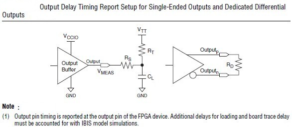
Diagrams