(China (Mainland))

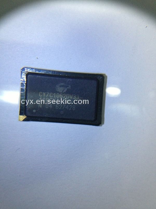
Product Summary
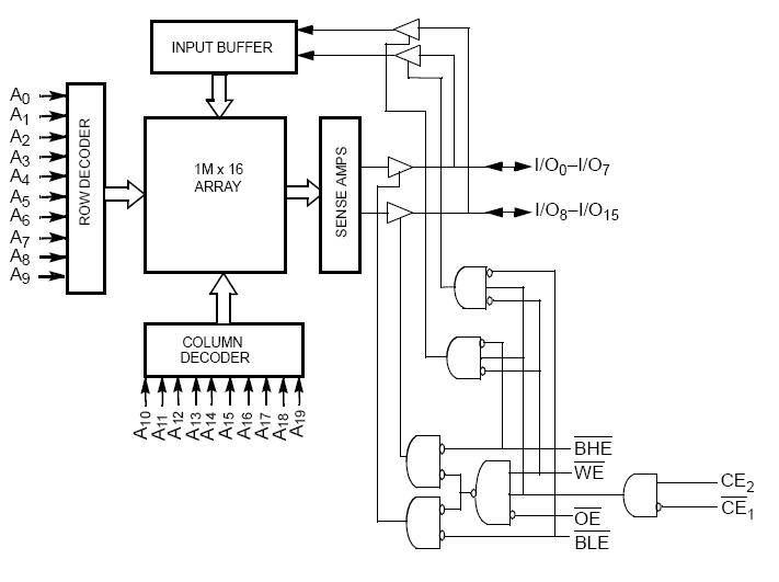
The CY7C1061DV33-10BGXI is a high-performance CMOS Static RAM organized as 1,048,576 words by 16 bits. Writing to the CY7C1061DV33-10BGXI is accomplished by enabling the chip (CE1 LOW and CE2 HIGH) while forcing the Write Enable (WE) input LOW. If Byte Low Enable (BLE) is LOW, then data from I/O pins (I/O0 through I/O7), is written into the location specified on the address pins (A0 through A19). If Byte High Enable (BHE) is LOW, then data from I/O pins (I/O8 through I/O15) is written into the location specified on the address pins (A0 through A19).
Parametrics
CY7C1061DV33-10BGXI absolute maximum ratings: (1)Storage Temperature:–65℃ to +150℃; (2)Ambient Temperature with Power Applied:–55℃ to +125℃; (3)Supply Voltage on VCC Relative to GND[2]:–0.5V to +4.6V; (4)DC Voltage Applied to Outputs in High-Z State[2]:–0.5V to VCC + 0.5V; (5)DC Input Voltage[2]:–0.5V to VCC + 0.5V; (6)Current into Outputs (LOW): 20mA; (7)Static Discharge Voltage: >2001V (per MIL-STD-883, Method 3015); (8)Latch-up Current: >200mA.
Features
CY7C1061DV33-10BGXI features: (1)High speed: tAA = 10 ns; (2)Low active power: ICC = 125 mA @ 10 ns; (3)Low CMOS standby power: ISB2 = 25 mA; (4)Operating voltages of 3.3±0.3V; (5)2.0V data retention; (6)Automatic power-down when deselected; (7)TTL-compatible inputs and outputs; (8)Easy memory expansion with CE1 and CE2 features; (9)Available in Pb-free 54-pin TSOP II package and 48-ball VFBGA packages.
Diagrams